
Downloads: Sprint Layout 5.0 (Demo)
Sprint Layout 5.0 (Demo)
|
+ Download |
 Δημιουργός
 Μέγεθος
 Downloads
Ενα μικρό και εύκολο πρόγραμμα σχεδιασμού, τυπωμένου κυκλώματος/πλακέτας εως και 4 επίπεδα (4 Layers), με επαγγελματικές ικανότητες.
Αυτό που το κάνει να ξεχωρίζει απο τα άλλα, είναι η δυνατότητα που έχει, να "αντιγράφει" το τυπωμένο απο ένα αρχείο Bitmap.
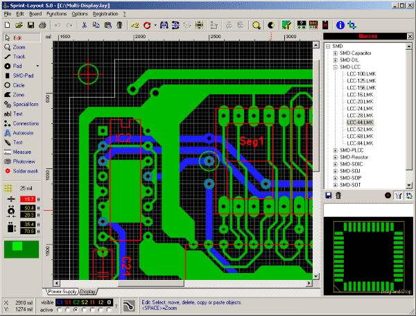

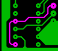
Sprint-Layout is equipped with tools to draw pads, tracks, copper areas, labels and so on. Just select the corresponding mode and place your elements. All parameter like track-width, pad-size, etc. are always visible at a glance, and can be edited every time. The active grid-capture lets you easily place your elements exactly.
You can edit existing layout-elements very easy. For example if you adjust the width of a track, you will see the result immediately on your layout. Additional functions like copy, move, rotate, mirror, etc. are self evident.
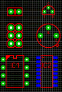
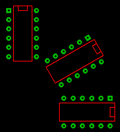
Component-library
Components which you have drawn once, can be added to the component-library. The component-library is already filled with many common used components. So you don’t have to create them again.
You can easily drag&drop the components from the library to your layout. After that you can mirror, rotate or label them like you want.
You can add as many components as you want to the library. You can even sort and group the library, so you can create your own library.
Free rotating
You can rotate all components or elements in any angle. This makes it possible to place your components in the best manner.
Automatic Ground-Plane
This function fills unused areas of a layout with copper automatically. This accelerates the corroding process and saves corroding material. You may also use this function to create a screen for HF-boards.
You can also define thermal-pads on the automatic ground-plane.

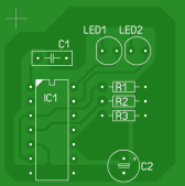
The Photoview
The photoview lets you take a look at your board as if it was already manufactured, with drillings, silk screen, etc. This helps you to find typically mistakes like wrong mirrored components or text.
You can select which board-side do you want to view and display or hide the silk-screen. With the “x-ray” feature you can make the board transparent, so that you can see the other board-side shine through.
Test-function
This function is very helpful to check your layout. You can click on any position of your layout, and Sprint-Layout will find all connected layout-elements, and light them up. This makes it very easy to check the signal flow of the layout.
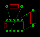
Connections (Rubberbands)
With the help of this connections, you can simplify the routing process. Straight rubberband lines are used to indicate connections that have not yet been routed. This may help you not to forget any tracks. The rubberband lines are also helpful to find a suitable position for components. You may use them to avoid crossing tracks when placing the components on the board.
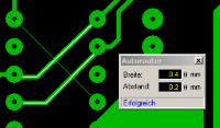
The Autorouter
There is simple point-to-point autorouter integrated in Sprint-Layout. This autorouter is able to connect two points of your layout. These two points are defined with a connection (rubberband). The autorouter was not designed, to generate whole boards at once. This is usually not possible. To create a proper layout, you have to design it mostly by yourself.
The autorouter in Sprint-Layout is designed as an easy to use autorouter. You don't have to make obscure specifications and options. The autorouter is as simple as the whole software.
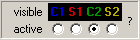
Layer administration
Sprint Layout offers - for both sides of the board - a copper- and a silk-screen-layer. Optional there are 2 inner layers (for multilayer PCB’s) and an outline layer (for the outline of your board) available. The layers can be switched on and off whenever necessary.
Several boards
A Sprint-Layout file can contains several boards. So you can add all boards of a project to one file. With a single click you get access to any board of your project.
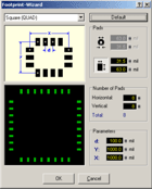
The Footprint-Wizard
The footprint-wizard helps you to create special footprints for components. You can specify the footprint-type and the parameters and the wizard creates your footprint automatically.
Every footprint-type has different parameters. These parameters are displayed and explained in a little picture in the footprint-wizard.
All changes that you made will be displayed in the preview immediately. If you have set all parameters, the footprint-wizard creates the footprint and you can place it on your layout.
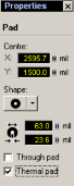
Properties-Panel
The properties-panel offers the possibility to edit all important properties of your layout-elements without calling special dialogs. Besides you can edit here special properties like positions, etc.
The properties-panel responds on the current selection on your layout. If you select e.g. a single pad, you can edit its properties directly here.
In the same manner, you can edit all other elements like tracks, text labels, etc.
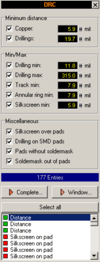
Design-Rule-Check (DRC)
Because of little inaccuracies while a PCB will be produced, there are some tolerances and limitations to keep, to get a usable Board. These values are named "Design Rules". Sprint-Layout is able to check some important design rules, e.g. the minimum clearance distance between 2 copper tracks, etc.
After a DRC is finished, all detected problems are listed in clear text and the problem-areas will be marked with a white hatch. Now you can examine the problems one after the other and correct them.
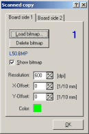
Scanned copies
Scanned layouts (e.g. from magazines) may be used as a copy for reproduction or for simple extensions. The layout must be available as a bitmap file. The bitmap is displayed in the background of the editor.
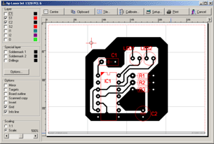
Printing
Various options are available to print your layouts, solder masks, component-mounting-plans, silk-screens or drilling-plans on paper sheets or transparent film.
The printout position is adjustable and the tile-option allows you to repeat the printout of small designs in x- and y-direction, to save film and material.
The printout can be scaled.
All changes you make will be displayed in the preview immediately.
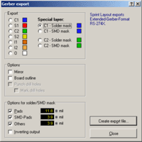
Gerber / Excellon export
Sprint Layout produces GERBER files (RS-274X) that are used to exchange layout data with PCB manufacturers. Gerber files are common to (almost) all manufacturers. So you don’t need films or something else to produce your boards.
The drillings can be exported in the common EXCELLON format. With this feature you can drill your board automatically.
There are many PCB-manufacturer, which accept Sprint-Layout files (*.LAY) in a direct way, so you don’t have to create Gerber or Excellon files by yourself.
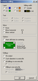
Isolation-milling
Sprint-Layout supports also the isolation-milling. In this case, the PCB will be produced using a CNC-milling machine. Sprint-layout is able to calculate all necessary isolation-channels. The output file will be exported in the HPGL format. You can use these files to load them into your milling-application and produce the board.
Additional functions like drilling-outputs, mirroring or the option to define texts as singleline or outline, give you numerous possibilities.
You can also define so called “reference holes”. This feature guarantees the same origin if you have several milling-jobs.
Εικόνες
")
Σχόλια
|
sakisr
18-05-11 at 00:05
|
Ευχαριστώ πολύ!!!!Χρησιμότατο! |
|
nikos.m5
02-07-11 at 04:07
|
Ευχαριστώ!!!! |
|
steliosb
22-07-11 at 09:45
|
Ευχαριστώ !!! |
|
martin27
28-07-11 at 16:23
|
Είναι φανταστικό ευχαριστώ πολύ!!!!!!!!!!! |
|
panosmag
20-12-11 at 17:54
|
Ευχαριστώ πολύ |
|
nickbaz
31-01-12 at 21:39
|
ευχαριστώ!!!!! |
|
aris k
21-02-12 at 19:04
|
ευχαριστω πολυ |
|
soloragr
20-03-12 at 21:03
|
Ευχαριστώ πολύ |
|
manousos81
28-05-13 at 13:40
|
Ευχαριστώ ..... |
|
mpempis100
03-02-14 at 21:07
|
ευχαριστω |
|
geotron
15-12-14 at 19:48
|
ευχαριστω πολυ |
|
gregoris
31-01-15 at 12:27
|
Ευχαριστώ φιλε |
|
johnis9300
06-05-18 at 16:15
|
ευχαριστω |
